Valve Index HMD detailed teardown
If you have ever wondered what is inside Valve Index, you might have stumbled upon my reddit post from 2019. I’ve decided to dive into the details of what makes Valve Index great and share my thoughts on tech inside.
Teardown should begin from the simplest parts - remove the face mask (held by just magnets), unplug the main cable, and remove headphones that are held in place by a single screw each. Next remove the rubber cover that is glued around lenses. It’s not that well glued, you can just pull it off.
 Rubber cover that prevents dust from getting inside lenses
Let’s start with a front panel - glossy front panel is removed by hand, since it is only held by magnets (but you already knew that from all the numerous pictures of people shoving stuff in the frunk of the headset). The rest of the front panel can be easily split in two parts. First is the frunk section, it will give you access to the main circuit board of the headset. You can remove it quite painlessly if you have the correct screwdriver. This panel does not contain any electronics.
 Just look at this beauty
Second part of the front panel is more complex. It contains tracking points for the SteamVR tracking - you can see them by looking at the plastic at different angles - plastic covering tracking points is thinner so laser beams from base stations could shoot through it. SteamVR trackers are split in two independent parts, which are connected to the main circuit separately. Also this panel contains two front facing cameras, which makes the process of taking it off even more delicate. You have to disconnect two cameras and two halves of the tracking plate’s system to finally fully reveal the main circuit.
Main Circuit
 The “meat” of Valve Index
Finally we get to the main computing power of the headset. You can identify the main points of the headset.
 This is where all the cables connect to the HMD
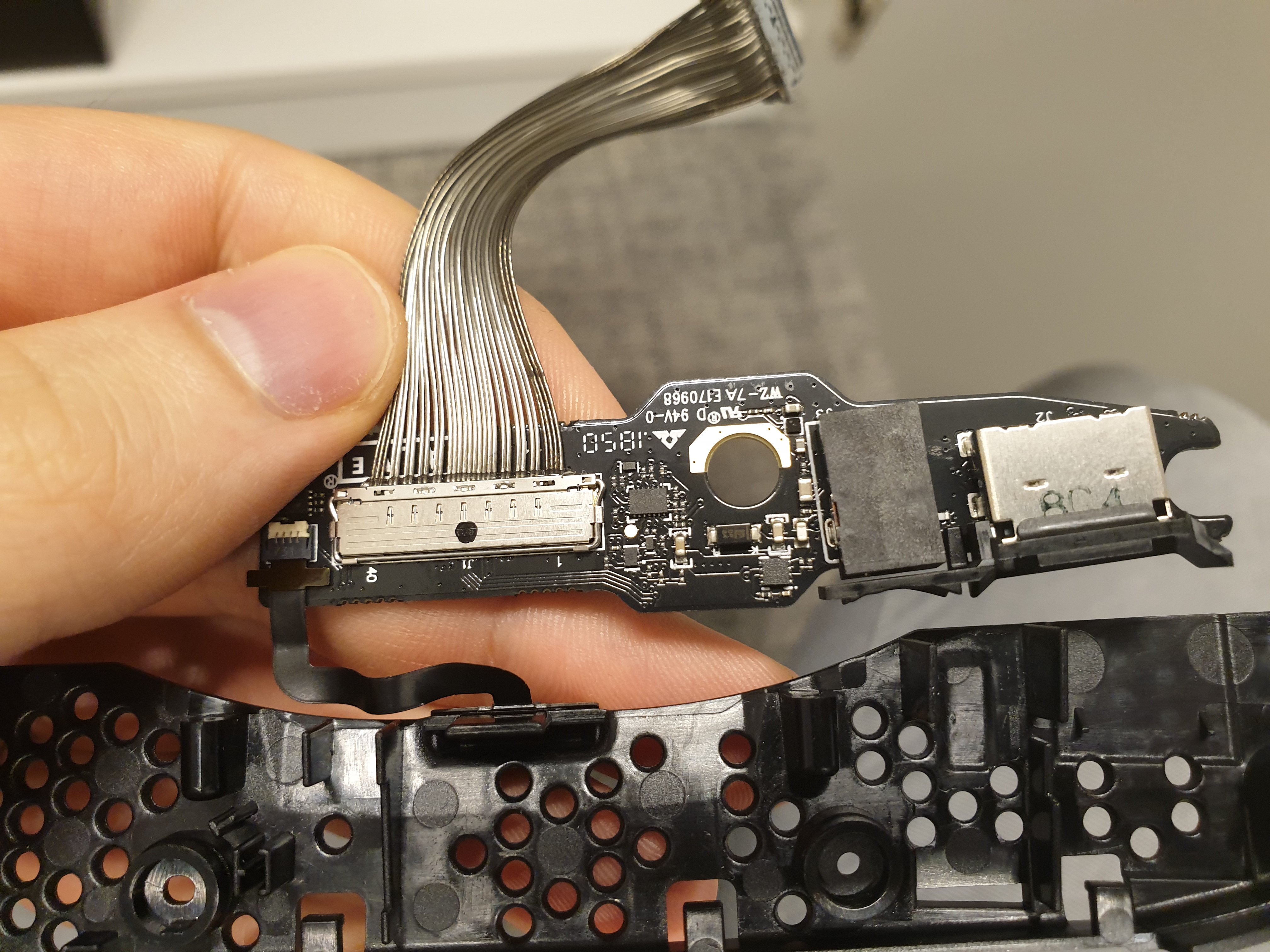
On the top there is a metal connector with FPC cable going in. It is going to the smaller circuit in the top part of the headset where the cable plugs in the headset.
 Circuit board with main cable and 3.5 mm audio port. It also connects to the proximity sensor
Same circuit has a 3.5 mm audio port for connecting headphones (I bet you didn’t know there is an audio jack) and proximity sensor between lenses. Last one is used for turning off the screens when the headset is not on the head.
 SteamVR tracking points are connected here
On the sides of the main circuit board there are two black FPC cables. Those are going to the SteamVR tracking dots located in the sides of the headsets. Here is a picture of the tracking “web” when taken out of the headset.
 One side of SteamVR tracking web taken out of the HMD
Final two FPC cables are orange color and located at the bottom of the main board. They are connecting to a pair of displays located right behind this circuit.
Microchips
Now it is time to dive in a wonderful world of microchips and circuit boards. I want to thank Sergejs Popovs for helping to identify most of the components on the board.
Let’s start with simple chips. Here are two bluetooth chips from Nordic Semiconductors. Each of these chips is used for connecting one controller with the headset. That’s why there is a limitation of two devices connected to the HMD. If you want to connect more devices (Vive Trackers or other controllers) you will need to use a USB dongle with a separate Bluetooth chip.

 Bluetooth microchips, each connects to one device
Do you remember the USB port in the frunk? Well, this is a chip from Microchip for that USB port - hence USB in the name.
 USB chip for USB port next to it
Here is a chip from Via-Labs. It has a purpose of converting USB 3.1 signal to the 2.0 one. Some of the chips on the circuit are not advanced enough to understand 3.1 USB, so this chip “dumbs it down”. When the signal will need to go back to the PC, the chip will convert the signal back to the USB 3.1.
 USB signal converter chip
This is a flash memory chip from Winbond Electronics.
 Flash memory can be used for different kinds of tasks
Next are these two microchips. The smaller one is a SlimPort® 4K receiver from Analogix. It is capable of receiving Image in 4K at 60 Hz, but since screens in Valve Index are only 1440 by 1600 pixels it allows to process video at 90, 120, and even 144 Hz. It also splits the signal in two allowing each display to get its own image.
 Video chips convert image that you see in your SteamVR mirror in beautiful VR image
Larger chip is a multipurpose FPGA (Field Programmable Gate Array) chip from Lattice Semiconductor. It is used for tracking - all the data received from the tracking sensors is gathered here. This chip combined with the Atmel MCU (located on the other side of the circuit board) are doing all the necessary tracking calculations.
EtronTech microchip is used for merging video feeds from external cameras and transmitting it to your PC.
 Microchip for processing image from webcams
Last two chips on this side of the circuit from SiliconLabs are most likely related to power regulation. Both of them are located near the capacitors and an inductor (metal thingy with 150 written on it). These are making sure that nothing will get too hot on your face.

 Power regulating microchips
Next step is to remove the main circuit board and look on its other side. Other side is less interesting and has very little information to offer. Most parts are related to the power regulation mentioned in the previous paragraph.
 Back side of the main circuit board
Largest chip is an Atmel MCU, which I’ve already mentioned is related to the tracking system. On the left from it is a microcontroller from NXP. These are all the chips we managed to identify. One chip that is missing, is the additional Bluetooth module. Unlike Vive and Vive Pro, Index has bluetooth in the headset. It is used for connecting to the base stations, updating base station firmware, and sending them to sleep mode when the headset is turning off. Last one is completely optional - I prefer to keep my base stations 2.0 on all the time.
 The only two chips worth noting on this side of the motherboard - larger one is for tracking calculations
Why there is no separate Bluetooth chip for this purpose is still a mystery for me. Only possible explanation is that two Bluetooth chips for controllers are capable of switching to different modes and control the base stations.
Screens
After the circuit is removed you will reveal several key components. First - you can see two displays - quick search shows that those panels are made by BOE Technology - Chinese display manufacturer. Those are 1440×1600, 615PPI 3.5” panels.
 View of the HMD with main board removed
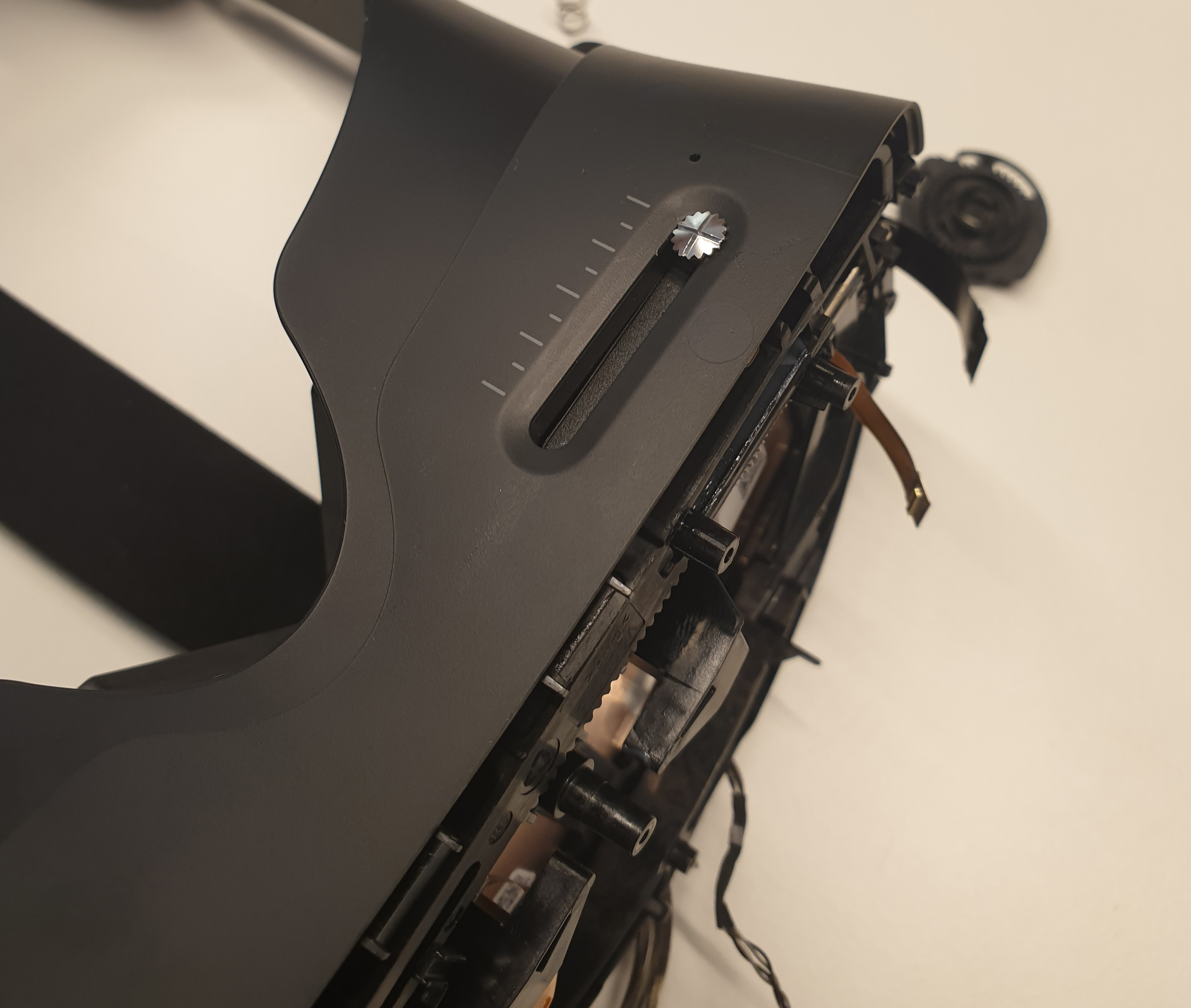
Note some key elements in this view. On the bottom there is a circular mechanism with a metal pin with springs going through the whole headset. Similar pin is barely visible on the top of the headset. This is an IPD adjustment system - movement of the knob at the bottom of the HMD will rotate circular element in the bottom center which will push screens apart. On the left and right sides of HMD you can see black gears - this is a system for eye relief - rotating a knob on the side of the headset will move the facemask relatively to the screens. Gear system is making sure both sides are rotating simultaneously, without giving too much pressure to the mechanism.
 IPD knob is actually a screw
In order to take the central part out from the headset, you will need to take the cap off the IPD adjustment knob and unscrew it.
 Lens chambers with IPD mechanism still attached
Next was what I call the “wondering in the dark” part of teardown - for about 30 minutes we were trying to find a way of taking it apart without breaking anything, eventually using force to break one gear inside that was holding display chambers in place.
 Right eye lens chamber removed
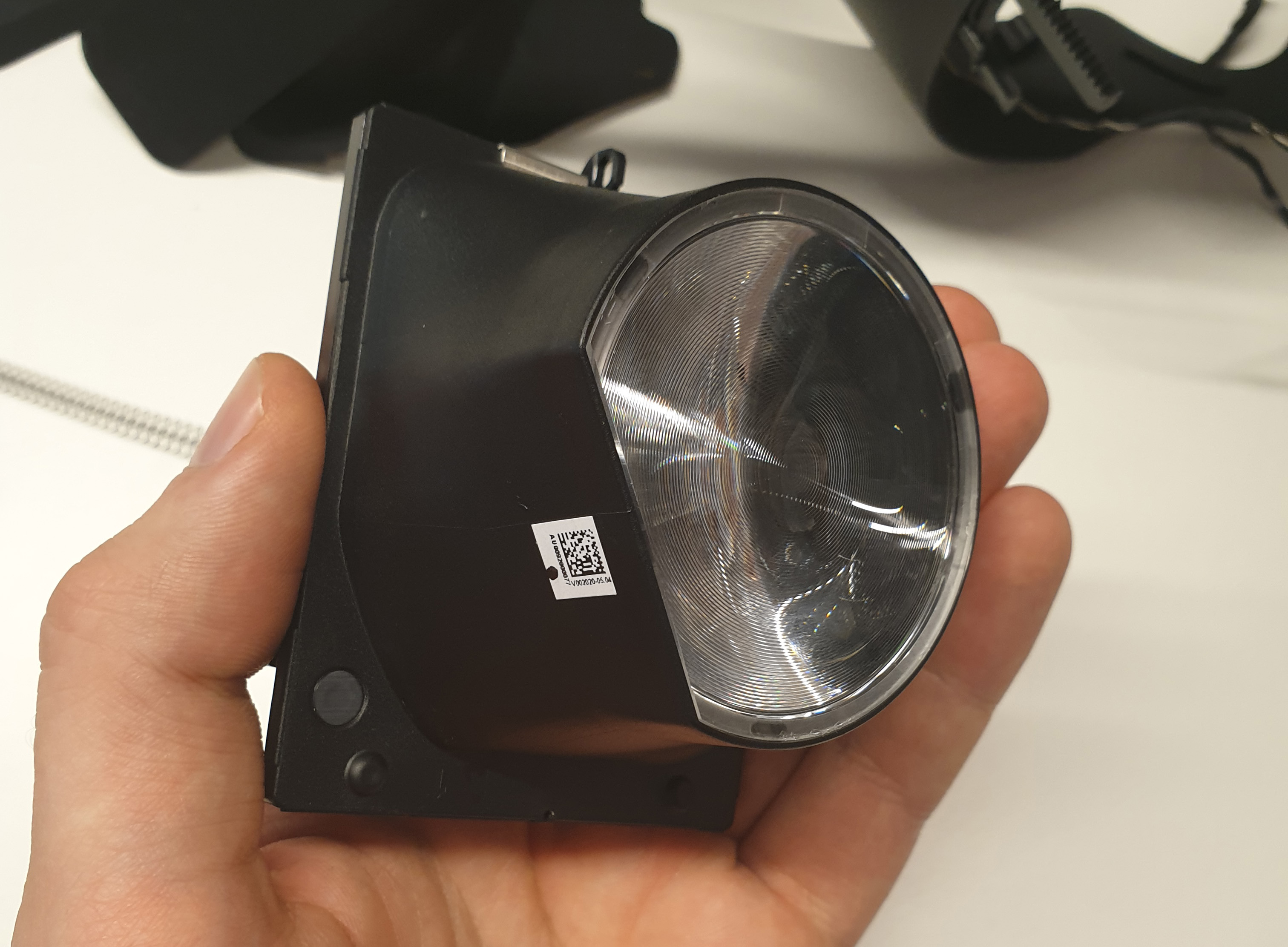
After this step you can easily take off separate lens chambers and view the details. Chambers are sealed shut so nothing will get inside - they are assembled in perfectly clean conditions with no dust particles. In order to take it apart you can probably try to melt glue or something like that. But we are no iFixit, we used good ol’ force. Here you can see the screen separated from the chamber.

 BOE screen removed from the chamber
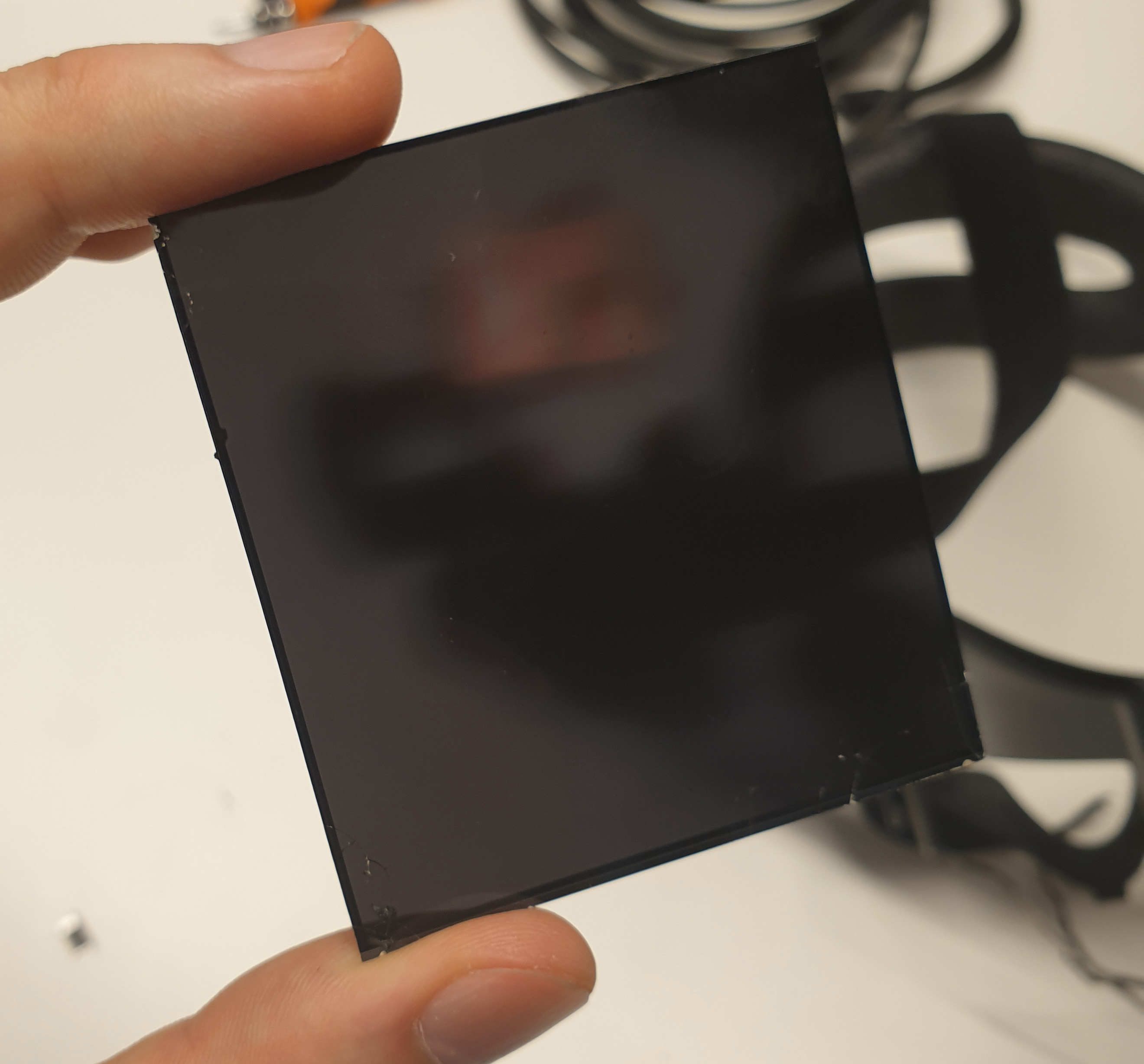
Screen has a polarised diffuser glued to it, which is particularly difficult to remove. It is made of very thin crystal glass and it cracks easily. You can see that the corners of it are cracked.
 Crystal polarisation diffuser
Diffuser is added to blend pixels better, making the screen door effect even lower.
 Fancy multilayered lens
Finally - the lenses. I was expecting them to be thicker with the effect that they create. Valve are saying “The custom lenses built into the Valve Index Headset maximize field of view without sacrificing edge-to-edge clarity. High geometric stability allows you to look around the scene by moving your eyes (not just your head) with minimal shape distortion”. I tend to agree that these are the most advanced lenses in modern mass produced HMD, even though they have their own flaws. Main issue is the light spill when using a headset, you can see the bright light’s reflections in spots where they shouldn’t be.
Final thoughts
As you can clearly see, it is not possible to replace a damaged screen or scratched lens all by yourself (even though for latter one you might try to take the lens out using a suction cup, however I don’t think that is a good idea, as lenses and screens are calibrated in the factory).
 Sometimes… I feel like a monster…
I am going to put the high-resolution images of the teardown and of the motherboard here so you can see and check all the details by yourself. If you have any corrections, notes, or questions, shoot me an email or PM me on Twitter.